Data Sheet, V2.1, Oct. 2006
BGF104
HSMMC Interface Filter and ESD Protection
Small Signal Discretes
�Edition 2006-10-17
Published by
Infineon Technologies AG
81726 München, Germany
© Infineon Technologies AG 2006.
All Rights Reserved.
Legal Disclaimer
The information given in this document shall in no event be regarded as a guarantee of conditions or
characteristics (“Beschaffenheitsgarantie”). With respect to any examples or hints given herein, any typical values
stated herein and/or any information regarding the application of the device, Infineon Technologies hereby
disclaims any and all warranties and liabilities of any kind, including without limitation warranties of
non-infringement of intellectual property rights of any third party.
Information
For further information on technology, delivery terms and conditions and prices please contact your nearest
Infineon Technologies Office (www.infineon.com).
Warnings
Due to technical requirements components may contain dangerous substances. For information on the types in
question please contact your nearest Infineon Technologies Office.
Infineon Technologies Components may only be used in life-support devices or systems with the express written
approval of Infineon Technologies, if a failure of such components can reasonably be expected to cause the failure
of that life-support device or system, or to affect the safety or effectiveness of that device or system. Life support
devices or systems are intended to be implanted in the human body, or to support and/or maintain and sustain
and/or protect human life. If they fail, it is reasonable to assume that the health of the user or other persons may
be endangered.
�BGF104
BGF104
Revision History: 2006-10-17, V2.1
Previous Version: 2006-03-03
Page
Subjects (major changes since last revision)
All
Layout conformation
Data Sheet
3
V2.1, 2006-10-17
�BGF104
HSMMC Interface Filter and ESD Protection
HSMMC Interface Filter and ESD Protection
Feature
• ESD protection and filter for High Speed Multi Media Card
interface
• ESD protection up to 15 kV at the external IOs
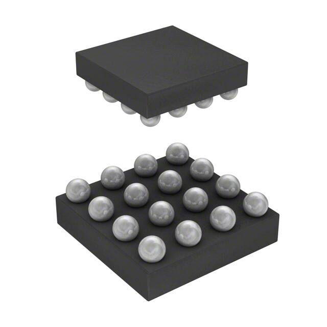
• 16 pin green wafer level package with SnAgCu solder
balls
• 500 µm solder ball pitch
• 300 µm solder ball diameter
WLP-16-1
R7, 75kΩ
R8, 75kΩ
R9, 75kΩ
R10, 75kΩ
Int. IOs
Ext. IOs
R11, 7kΩ
VMMC
V dd
A3
clk
A2
A4
MMCclk
R1, 50 Ω
B4
MMCcmd
R2, 50 Ω
cmd
A1
C4
MMCdat0
R3, 50 Ω
dat0
B2
C3
MMCdat1
R4, 50 Ω
dat1
B1
D4
MMCdat2
R5, 50 Ω
dat2
C1
MMCdat3
R6, 50 Ω
dat3
D1
D3
B3, C2, D2
GND
BGF104_schematic.vsd
Figure 1
Blockdiagram
Description
The BGF104 is an ESD protection and filter circuit for a high speed multi media card interface. External pins are
protected up to 15 kV contact discharge according to IEC61000-4-2. The wafer level package is a green package
with a size of only 1.96 mm x 1.96 mm and a total height of 0.65 mm.
Type
Package
Marking
Chip
BGF104
WLP-16-1
BGF104
N0708
Data Sheet
4
V2.1, 2006-10-17
�BGF104
HSMMC Interface Filter and ESD Protection
Table 1
Maximum Ratings
Parameter
Symbol
Values
Min.
VP
TOP
TSTG
Voltage at all pins to GND
Operating temperature range
Storage temperature range
Typ.
Unit
Note /
Test Condition
Max.
-14
14
V
-40
+85
°C
-65
+150
°C
-15
15
kV
-2
2
kV
Electrostatic Discharge According to IEC61000-4-2
VE
VI
Ext.IOs: A1, A2, A3, B1, B2, C1, D1
Int. IOs: A4, B4; C3, C4, D3, D4
Table 2
Electrical Characteristics1)
Parameter
Symbol
Resistors R1...R6
Resistors R7...R10
Resistor R11
Reverse current of ESD protection diodes
R1...6
R7...10
R11
IR
Values
Min.
Typ.
Max.
40
50
60
Ω
52.5
75
97.5
kΩ
4.9
7
9.1
kΩ
5
0.1
100
10
nA
µA
16
20
pF
CT
Line capacitance
Capacitance of each line to GND
1) at TA = 25 °C
Unit
Note /
Test Condition
VR = 3 V
VR = 14V
VR = 0 V
R7, 75kΩ
R8, 75kΩ
R9, 75kΩ
R10, 75kΩ
Int. IOs
Ext. IOs
R11, 7kΩ
VMMC
V dd
A3
MMCclk
R1, 50 Ω
clk
A2
B4
MMCcmd
R2, 50 Ω
cmd
A1
C4
MMCdat0
R3, 50 Ω
dat0
B2
C3
MMCdat1
R4, 50 Ω
dat1
B1
D4
MMCdat2
R5, 50 Ω
dat2
C1
D3
MMCdat3
R6, 50 Ω
dat3
D1
A4
B3, C2, D2
GND
BGF104_schematic.vsd
Figure 2
Data Sheet
Schematic
5
V2.1, 2006-10-17
�BGF104
HSMMC Interface Filter and ESD Protection
1.96 ±0.05
0.65 ±0.05
B
0.1 C
0.5
A
A4
A3
A2
A1
B4
B3
B2
B1
C4
C3
C2
C1
D4
D3
D2
D1
0.5
16x
ø0.05 M A B
0.3 ±0.05 1)
1) D imension is measured at the maximum solder ball diameter, parallel to primary datum C
2) Pin A1 corner identified by marking
3) Primary datum C and seating plane are defined by the spherical crowns of the balls
0.25 ±0.1
8
2.42 ±0.05
Pin 1 Corner
Index Area 1)
2.42 ±0.05
1) Balls face down
Data Sheet
G W LN1057
Package Outline WLP-16-1
4 ±0.1
Figure 4
1.96 ±0.05
C
0.08 C
16x
C OPLAN AR ITY
Figure 3
3 x 0.5 = 1.5
0.5
SEATING PLANE
3)
Pin A1 2)
0.25 ±0.05
STAN D OFF
3 x 0.5 = 1.5
0.95 ±0.05
CWLG1065
Tape for WLP-16-1
6
V2.1, 2006-10-17
�